Position:Home » Technical Articles
Thin Film Resistor's Negative Etching Method and Lithography
Writer:Microhm Page View:Date:2019-04-17
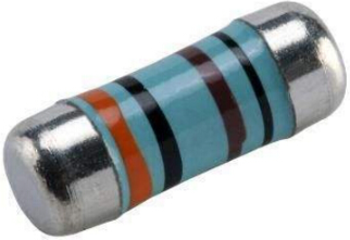
Thin film resistor is a kind of more common resistor. Usually the manufacturing method of thin film resistor includes insulating substrate, forming a conductor pattern layer on the insulating substrate by non-photolithography. A thin film resistance layer is formed on the conductor pattern layer and the insulating substrate. The thin film resistive layer is patterned by photolithography. This thin film resistor manufacturing method can reduce the manufacturing cost of thin film resistor, but at present, many thin film resistors choose negative etching method. This kind of thin film resistance manufacturing method is becoming more and more popular.
The "negative etching method" is often used to fabricate thin film resistors. The first photoetching and etching are carried out to obtain the whole pattern of electrodes and resistors, and then the resistance pattern is obtained by lithography and etching with the selective mask of the coated resistance mask. The biggest problem with this approach is that the registration window is narrow. Since the "alignment mark" is limited to the edge of a particular structure, it is not a guarantee of registration anywhere. Registration will be affected by lens distortion, abnormal clamping of ceramic plates, misalignment of mask patterns, and distortion of ceramic plates themselves.
Therefore, in order to fabricate thin film resistance by etching method of negative plate, we usually align the "alignment mark" between the cover mask and the upper layer of microstructure, and then observe whether the pattern on the two is correct or not, and if there is a misalignment, fine-tuning is carried out. After the full registration of the graphics, then do the exposure and other work.
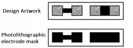
When ordinary contact or proximity lithography machine is used to cover the resistance,
once there is a chain reaction when the pattern is not set, and then the resistance pattern corrosion dislocation, the light one will cause a large deviation of the resistance value. The most important factor is that the microwave circuit pattern is destroyed, which directly affects the yield of the product. Therefore, in general, it is necessary to take timely rework when the misalignment is found in the mirror inspection, but the production efficiency is not high because of the cost of work and waste.
As can be seen from the above, the thin film resistance production method is very important, if the incorrect production method is adopted, there is a great difference between the precision and the production cost of the thin film resistance obtained by the incorrect production method. In addition, the fabrication of thin film resistors is an important step in the production of hybrid microwave integrated circuits, and the advantages and disadvantages of the preparation methods are also discussed. To a large extent, the production efficiency and yield of microwave integrated circuits are determined.
The "negative etching method" is often used to fabricate thin film resistors. The first photoetching and etching are carried out to obtain the whole pattern of electrodes and resistors, and then the resistance pattern is obtained by lithography and etching with the selective mask of the coated resistance mask. The biggest problem with this approach is that the registration window is narrow. Since the "alignment mark" is limited to the edge of a particular structure, it is not a guarantee of registration anywhere. Registration will be affected by lens distortion, abnormal clamping of ceramic plates, misalignment of mask patterns, and distortion of ceramic plates themselves.
Therefore, in order to fabricate thin film resistance by etching method of negative plate, we usually align the "alignment mark" between the cover mask and the upper layer of microstructure, and then observe whether the pattern on the two is correct or not, and if there is a misalignment, fine-tuning is carried out. After the full registration of the graphics, then do the exposure and other work.
When ordinary contact or proximity lithography machine is used to cover the resistance,
once there is a chain reaction when the pattern is not set, and then the resistance pattern corrosion dislocation, the light one will cause a large deviation of the resistance value. The most important factor is that the microwave circuit pattern is destroyed, which directly affects the yield of the product. Therefore, in general, it is necessary to take timely rework when the misalignment is found in the mirror inspection, but the production efficiency is not high because of the cost of work and waste.
As can be seen from the above, the thin film resistance production method is very important, if the incorrect production method is adopted, there is a great difference between the precision and the production cost of the thin film resistance obtained by the incorrect production method. In addition, the fabrication of thin film resistors is an important step in the production of hybrid microwave integrated circuits, and the advantages and disadvantages of the preparation methods are also discussed. To a large extent, the production efficiency and yield of microwave integrated circuits are determined.
Latest News
- Resistor's role in measuring and correcting LED,,,
- Single through-hole resistors' characteristics ,,,
- Why shunt resistors for current sense applicati,,,
- Metal-film resistors with small size, high resi,,,
- 36W High-Current Shunt Resistors MMS8420,,,
- 1W Surface Mount Resistor MPR1206,,,
- An Overview of Microhm Electronics' Resistor Pr,,,
- More anti-sulfur resistors used in harsh envir,,,
- Resistance changes with temperature,,,
- 140W TO247 High Power Heatsinkable Resistor,,,
- MMS5930 is ideal for current sensing in industr,,,
- Shunt resistors selection for engineers' design,,,
- Considerations for choosing precision resistors,,,
- Ceramic Encased Cement Resistors NWH Series for,,,
- Resistors for Passive Balancing in Battery-Pow,,,
Hot Articles
- Microhm will take part in 10th Automotive World,,,
- Thanks for Visiting Microhm's Booth E5-5706 in ,,,
- Resistors in Short Supply: Blame Cars,,,
- New lunch: High Power Precision Shunt Resistor,,,,
- How to Test a Resistor,,,
- Innovative Technology, Future Electric: Electri,,,
- What is Precision Resistors?,,,
- SMD Resistors Sizes and Packages,,,
- The Construction and Features of Metal Film Res,,,
- What is a TO-220 Resisor?,,,
- Hot Selling Products: Precision Shunt Resistors,,,
- How to Calculate the Equivalent Resistance Valu,,,
- What is a Fixed Resistor?,,,
- Resistors in LED Circuits,,,
- Resistors Types and Materials Overview,,,
Resistance applications
- Shunt Resistor MMS8420 for High Current Stable ,,,
- The Measurement Accuracy of Automotive Shunt is,,,
- Carbon Film Resistors' Features and Application,,,
- Select the Right Resistor for Harmonic Filterin,,,
- The Four Important Functions of Alloy Resistors,,,
- The Main Application for High Precision and Low,,,
- Industrial Roberts Applied to Solar Photovoltai,,,
- Why Zero-Ohm Resistors?,,,
- Difference Between High Precision Resistors and,,,
- Surface Mount Resistor's Size and Package ,,,
- Heater Blower Motor Resistor in Air Conditioner,,,
- Urbanization Development Bringing the Transform,,,
- Precision Resistors' Construction and TCR,,,
- Miniature future for passive electronic compone,,,
- BMS for New Energy Vehicle,,,